
By Dr Klaus Engenhardt
Architecture Lead
I recently joined a Signal Integrity Journal panel discussion on high-speed interconnect technologies, where industry experts shared their perspectives on the challenges ahead. The conversation highlighted several themes that I believe are critical to the future of interconnect test.
As high-speed interconnects move toward co-packaged optics, higher lane counts, and massively parallel architectures, test strategy is arguably becoming just as important as the interconnect technology itself. The challenge is not only to measure faster signals, but to test more channels, more consistently, and at a lower cost per channel as device complexity increases.
This represents one of the biggest shifts in high-speed interconnect test. Electrical and optical interfaces will coexist for the foreseeable future, and test systems will need to support both domains while keeping pace with the scale of future devices.
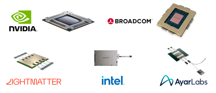
Testing challenges as lane counts increase
Today’s pluggable optical transceivers typically have a limited number of lanes. Future CPO optical engines, however, are targeting 32 or 64 transmit channels, and just as many receive channels. At that scale, traditional testing becomes a bottleneck.
“The sheer number of channels in future CPO optical engines demands parallel testing, where the test equipment’s channel count has to scale with the devices we’re trying to test.”
For manufacturing test engineers, the challenge is no longer only to make accurate measurements at higher bandwidths. It is to make those measurements across every lane and every channel, repeatedly and efficiently, without allowing test cost to grow linearly with channel count.
Cost of test becomes a scaling challenge
High-frequency broadband test equipment is expensive, and it can quickly become a limited resource. A company cannot simply keep adding more 110 GHz VNAs, sampling oscilloscopes, or other high-end instruments every time the number of lanes increases. This problem becomes more critical as channel counts rise.
In manufacturing test, especially for emerging technologies that are not yet mature, every lane and every channel needs to be tested. The challenge is not just scaling the channel count, but reducing the cost per channel at the same time.
This is why scalability has become an important consideration in high-density test system planning. A high-density test system needs to add channels efficiently, support parallel measurement where it delivers the greatest benefits, and deliver consistent performance as the system grows.
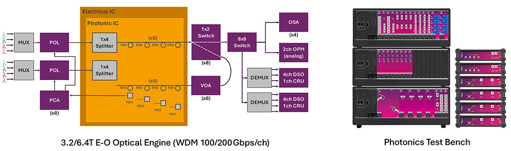
Multi-domain testing across electrical and optical interfaces
The future of high-speed interconnects will not be purely electrical or purely optical. Signal paths increasingly span electrical and optical interfaces, while validation activities may occur at the wafer, die, package, module, and system levels.
Addressing these challenges requires test capabilities that support the full spectrum of interconnect technologies, from backplanes, copper cables, ACCs, AECs, and AOCs through to transceivers, near-packaged optics, and co-packaged optics.

No single test approach addresses every stage of this ecosystem. Different technologies require different measurement techniques, from high-speed I/O characterization and channel analysis to active alignment, optical device characterization, and end-to-end interconnect validation.
As systems become more complex, the challenge is not only achieving measurement performance within each domain, but building test strategies that provide consistent and actionable insight across the product lifecycle.
Repeatability matters as much as scale
Increasing channel count alone is not enough. If measurements vary significantly from one channel to another, the value of parallel testing is reduced. Test engineers need confidence that differences in the results reflect the device under test, rather than variability in the test setup.
That makes calibration, channel-to-channel correlation, and system-level repeatability essential parts of any high-density test strategy. Better measurement consistency helps reduce variability, and that ultimately supports better manufacturing margins.
Designing for scalable manufacturing test
A lot of this also comes down to design for manufacturability. Built-in test capabilities, wafer-level access, and die-level test structures can help move testing upstream, so known good die can be identified before assembly. That is one of the ways the industry can begin to manage the cost of test as devices become more complex.
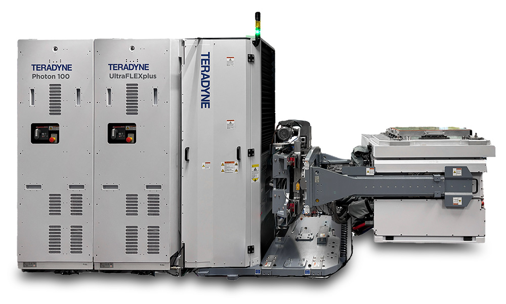
The broader point is that high-speed interconnect test is becoming a system-level challenge. Bandwidth and measurement accuracy still matter, but they are no longer the only considerations. The next generation of interconnects will require test strategies that scale across channels, domains, and manufacturing environments while keeping cost and variability under control.
From a Teradyne perspective, the challenge is not simply measuring faster signals. It is enabling scalable, cost-effective test strategies that help manufacturers increase throughput and accelerate the deployment of next-generation interconnect technologies.
Click here to watch the Signal Integrity Journal web panel discussion on demand
Have a test challenge you’d like to discuss?
We’re very interested to hear from anyone who is evaluating their high-volume testing options. Please reach out at sales@quantifiphotonics.com or contact us.
We’re also at ECOC 2026 – come see the Quantifi Photonics team at booth 2118 from 21-23 September in Malaga.
We’d love to see you there!