


Why Scalable Photonics Test Is Essential for Photonic Integrated Circuits and Co‑Packaged Optics
Photonic integrated circuits (PICs) and co‑packaged optics (CPO) are enabling the next generation of AI training clusters, high‑performance computing, and hyperscale data center architectures. However, these technologies cannot scale into high‑volume manufacturing until photonics testing itself can scale.
Unlike electronic IC test which was built around automated, wafer‑level workflows, photonics test evolved in low‑volume laboratory environments, creating fundamental throughput and cost‑of‑test limitations as devices move from the lab into production.
This perspective reflects Quantifi Photonics’ experience supporting scalable test strategies for photonic integrated circuits and co‑packaged optics as they transition from development into high‑volume manufacturing.
Scalable photonics test refers to test architectures and workflows that maintain throughput, correlation, and cost‑of‑test as photonic devices scale in channel count and move into high‑volume manufacturing.
On this page:
- Why can’t photonic integrated circuits (PICs) and co‑packaged optics (CPO) be deployed at scale today?
- What makes photonics testing fundamentally different from electronic IC testing?
- Why is parallel test essential for scalable PIC and CPO manufacturing?
- What is the “test funnel,” and why does shift‑left testing matter?
- How does modular test architecture enable continuity from lab to factory?
- What does parallel photonics test look like in production?
- Why does scalable photonics test require ecosystem collaboration?
Why can’t photonic integrated circuits (PICs) and co‑packaged optics (CPO) be deployed at scale today?
Photonic integrated circuits (PICs) and co‑packaged optics (CPO) are becoming foundational for AI training clusters, high‑performance computing, and hyperscale data centers because they enable higher bandwidth density and lower power consumption than copper interconnects. However, the industry cannot deploy PICs or CPO at scale until it can test them at scale. Unlike electronic IC test, which benefits from decades of automation and standardized, high‑throughput workflows, photonics test evolved in low‑volume laboratory environments where precision and flexibility mattered more than throughput. As devices leave the lab and enter manufacturing, those legacy approaches become a limiting bottleneck rather than an enabler.
What makes photonics testing fundamentally different from electronic IC testing?
Electronic IC testing was built for wafer‑based manufacturing from the outset. In contrast, photonic devices introduce additional constraints that must be addressed simultaneously and at scale: repeatable optical coupling across many sites, electro‑optical validation at 100% coverage, sensitivity to temperature and mechanical variation, and rapidly increasing channel counts. As PICs and CPO devices become denser, traditional serial test methods no longer meet either throughput or economic requirements.
Why is parallel test essential for scalable PIC and CPO manufacturing?
Scaling photonics test is fundamentally a parallelization problem. Once devices incorporate more than a handful of optical paths, stimulating and measuring channels sequentially becomes impractical. Parallel photonics test architectures make it possible to:
- Perform full electro‑optical validation at wafer sort
- Support multi‑site design‑verification testing without exploding test time
- Validate optical engines and modules at full data rate across multiple lanes simultaneously
For PICs and CPO engines with 8, 16, or 32 optical paths, parallel test is essential for manufacturing‑scale throughput.
What is the “test funnel,” and why does shift‑left testing matter?
Scalable photonics manufacturing relies on a structured test funnel that aligns test depth with each stage of the product lifecycle:
- Early development and characterization require broad visibility using passive, active, and high‑speed measurements to understand device behavior.
- Design verification testing (DVT) shifts the emphasis to automated, repeatable testing across process, voltage, and temperature.
- High‑volume manufacturing (HVM) depends on a much smaller, predictive test set that screens for yield and reliability.
Testing more extensively early in the development cycle enables aggressive reduction of test time downstream. This “shift‑left” approach is a practical requirement for cost‑effective, ultra‑high‑volume manufacturing of PICs and CPO.
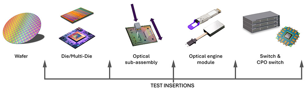
How does modular test architecture enable continuity from lab to factory?
Modern modular test architectures allow the same measurement hardware to be used across development, design verification, wafer sort, and module‑level test. A power meter or optical instrument initially used on a benchtop can later appear in a multi‑site DVT system and eventually in an automated production cell.
Maintaining consistent instruments, APIs, and data structures preserves correlation across the product lifecycle. This continuity eliminates the need to reinvent test infrastructure at each transition and accelerates yield learning as devices move into volume production.
What does parallel photonics test look like in production?
In manufacturing environments, parallelism becomes economically mandatory:
- Wafer‑level test combines electrical probing and optical coupling in parallel to enable efficient known‑good‑die workflows for silicon photonics.
- Module‑level and optical‑engine test validates assembled systems under thermal load and at full data rate, exercising multiple lanes simultaneously to evaluate eye quality, bit‑error rate, and receiver sensitivity.
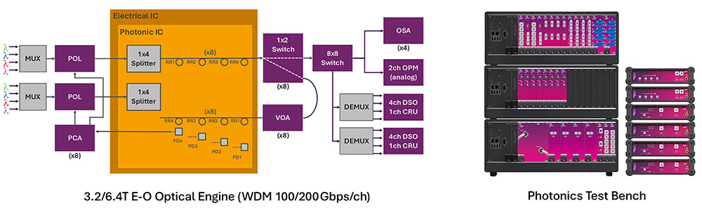
- For next‑generation 3.2T‑ and 6.4T‑class optical engines, this level of parallel testing is a hard requirement for cost‑effective, high‑throughput manufacturing.
Why does scalable photonics test require ecosystem collaboration?
Scaling photonics test is not a single‑vendor problem. Achieving semiconductor‑class throughput requires tight integration between optical instrumentation, ATE‑level automation, device handling, probing, and precision alignment technologies. When these elements operate as a cohesive system, manufacturers can maintain consistent test strategies from wafer to module to final package.
This ecosystem‑level cooperation is essential for creating the discipline, correlation, and predictability needed to move PICs and CPO from specialized engineering efforts into reliable, high‑volume production.
Key takeaway
According to Quantifi Photonics experts, test is no longer just a checkpoint at the end of the line. We believe it is a design constraint and a source of significant competitive advantage.
Devices will continue to add channels, operate at higher speeds, and dissipate more power. Manufacturers that adopt parallel, modular, and manufacturing‑grounded test strategies early are best positioned to scale photonic interconnect technologies for the next generation of AI and high‑performance computing systems.
To speak with an expert about developing a scalable test strategy, contact us.