


By Iannick Monfils, Chief Technology Officer,
Quantifi Photonics
For bandwidth-intensive computing applications such as data centers and machine learning and AI devices, bandwidth demands for these networks are rapidly increasing from 200G to 400G today and will soon be pushed to 800G and beyond. To help companies meet these speed and bandwidth demands, optical transceiver manufacturers need to develop transceivers that increase capacity without increasing device footprint and power consumption.
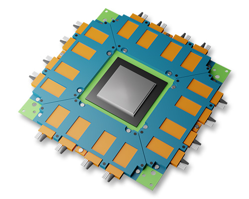
To address these seemingly conflicting demands, many optical transceiver designers are looking towards co-packaged optical technology. In short, co-packaged optical systems integrate optical engines with signal processing ASICs and other photonics elements on a packaged substrate. In this new form factor, the active device and optical transceivers are mounted on the same densely packed substrate, eliminating the loss and distortion typically experienced when multiple components are externally connected. The result is exactly what these applications need – an optical transceiver with greatly increased capacity and bandwidth that does not increase footprint and simultaneously decreases the total power consumption per bit.
Guidelines and specifications for co-packaged optical systems
To ensure continuity and interoperability of co-packaged optical devices, organizations such as the Optical Internetworking Forum (OIF) and Consortium for On-Board Optics (COBO) are currently iterating on framework and specification documentation for manufactures of these devices. At a high-level, the OIF framework is focused on addressing the application spaces and relevant technology considerations for co-packaging of optical and electrical communication interfaces. This framework includes guidance on how to design devices to reduce power consumption as bandwidth requirements increase, and how to use external laser sources, such as external laser small form pluggables (ELSFP), to extend the reliability and longevity of co-packaged optical devices. The purpose of the COBO specification is to provide common specifications for system manufacturers and integrators, component manufacturers, and suppliers of 8-lane and 16-lane on-board optics to ensure a consistent platform for end users of this technology.
Addressing testing challenges to develop in-spec co-packaging devices
As the standards above speak to, co-packaged optical devices have a channel density unlike any subassembly ever developed, which means existing test solutions cannot possibly be sufficient. For example, a 51.2 Tbps co-packaged optical device has 16 units of 3.2 Tbps modules, with each module having 8Tx and 8Rx fibers with 4 wavelengths per fiber. In total, this single co-packaged optical device has 512 channels, each operating at 100 Gbps. There are also several qualification tests required for each channel, and each test can be quite complicated since channels are likely using a multifiber construction and carrying multiple wavelengths.
With this large number of channels on a single device under test (DUT), production test engineers are facing several unprecedented testing challenges with co-packaged optical devices. One overarching challenge is that today’s optical test equipment is largely designed for R&D testing as it is both extensive in acute specifications and expansive in size. To perform the many tests required for a co-packaged optical device without taking months to verify a single DUT, manufacturers need an optical testing solution capable of rapidly performing mass parallel testing, much like electrical semiconductor testing is done today.
While it seems like optical testing capabilities are currently light years behind this type of semiconductor electrical testing, we are changing this. With our new PXI-based BERTs, new high-channel-density power meters, and new switches that can handle high fiber channel counts, we are helping manufacturers break through traditional optical testing bottlenecks by providing the highest test channel density products available for optical testing all in an open, scalable format.
The PAM4 BERT is built on open, modular, proven PXI technology and includes up to 8-channels per two-slot PXIe module. Each single PXIe mainframe can fit up to 64 synchronized channels, providing extremely high channel density of up to 256 channels. Our PAM4 BERT also inherently addresses the space limitations most transceiver manufacturers face as it is the smallest physical BERT on the market. Similarly, our new 288-channel high-density power meter provides 10X more density over current solutions, enabling rapid and highly parallel transmit and receiver channel calibration in a small form factor.

Enabling unprecedented density for optical transceiver test
At Quantifi Photonics, we are laser-focused on solving the numerous challenges involved in achieving the extremely high-bandwidths required to power the data-intensive devices we all rely on each day. With test equipment such as our new PXI-based high-density transceiver test systems and our high-channel count optical power meter, production test engineers can scale testing with small form factor test equipment, reduce testing complexities, decrease test times, and accelerate time to market.
Since bandwidth needs will continue to rapidly increase, we have intentionally designed our PAM4 BERT to scale to meet these needs and have a strong product development roadmap in place to address the optical testing challenges ahead. We are always happy to discuss the challenges device manufacturers are experiencing, especially as new industry frameworks and specifications are solidified. Our goal is to develop the testing solutions today that will meet tomorrow’s market needs.
Never miss a post
Subscribe to our blog to stay up-to-date on our latest innovations in photonics test and measurement.
